


How can a miniaturized laser be utilized?
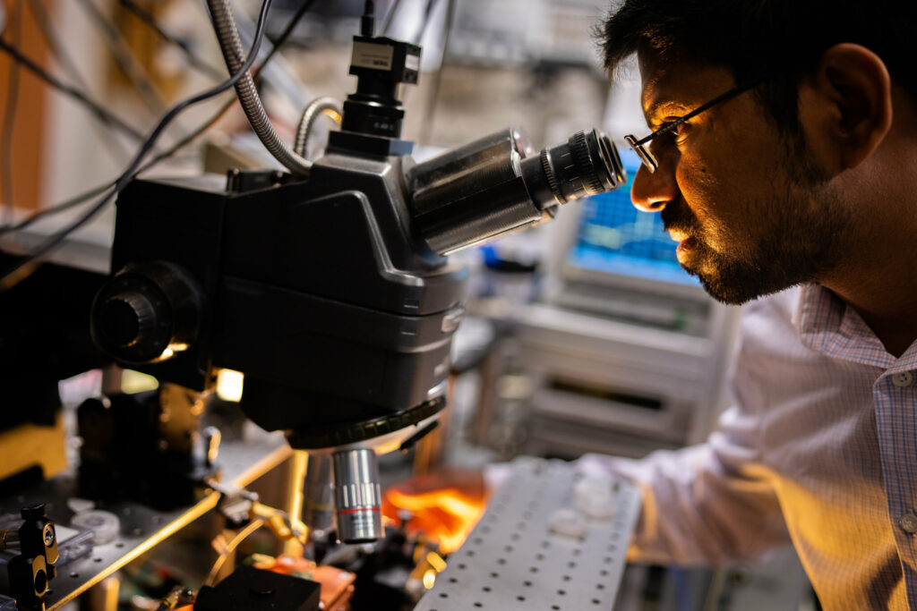
The laser is so minute that a microscope is required for proper observation. However, scientists at Sandia National Laboratories are not merely enthused about its size; the excitement stems from the laser’s potential integration with other microscale optical devices, promising advancements in various applications such as enhancing safety in self-driving cars, increasing efficiency in data centers, enabling portability in biochemical sensors, and enhancing versatility in radars and defense technologies.
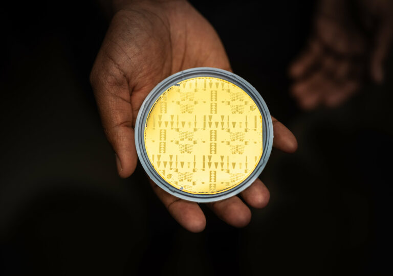
Sandia has secured a patent for its innovative approach to integrating diverse materials onto silicon—the foundational material used in semiconductor fabrication plants for microchip production. This technique empowers Sandia to construct high-bandwidth, high-speed optical devices, encompassing indium phosphide lasers, lithium niobate modulators, germanium detectors, and low-loss acousto-optic isolators—essential components for high-power optical systems. The remarkable feat of building a laser on silicon presents a challenging endeavor, showcasing the potential to extend America’s leadership in semiconductor technology.
While other entities, such as the University of California, Santa Barbara, and Intel Corp., have created similar lasers, Sandia distinguishes itself by expanding the array of devices that can be integrated. Notably, these devices can collaborate on optical microchips, also known as photonic integrated circuits, marking a pioneering development. Patrick Chu, co-leader of the National Security Photonics Center at Sandia, emphasized the significance of this achievement, stating, “This allows the U.S. to lead and have less dependency on foreign manufacturing capabilities.” Chu leads a group of over 60 photonics scientists and engineers at Sandia’s Microsystems Engineering, Science, and Applications complex.

Integration with silicon a key step toward future production
Silicon serves as the essential backbone of the semiconductor industry and is highly favored for crafting computer chips. Nonetheless, as noted by Ashok Kodigala, a research scientist at Sandia and one of the co-inventors of the innovative integration process, silicon alone is inadequate for laser manufacturing. The task at hand involved creating a method for harmonizing optical components made from diverse materials on a silicon microchip. Since these materials cannot be simply affixed in place, Kodigala ingeniously bonded them to silicon in intricate layers, employing a process known as heterogeneous integration.
The Sandia team effectively showcased heterogeneous integration methods, showcasing the creation of hybrid silicon devices. These include hybrid lasers and amplifiers constructed from both indium phosphide and silicon, along with modulators comprised of both lithium-niobate and silicon. The modulators play a crucial role in encoding information in light produced by the lasers. Additionally, high-power and high-speed germanium detectors were engineered to match the capabilities of the lasers and modulators within the same platform.
Semiconductor fabs could use Sandia technique
Sandia developed its chip-scale lasers with the aim of transitioning the technology to the industry. Leveraging tools akin to those found in commercial semiconductor plants, the team created lasers that emit light in wavelengths commonly utilized in the telecommunications sector, known as the C-band and the O-band. “After successfully showcasing this photonic platform at a national lab, we can subsequently transfer this technology to U.S. companies, enabling them to concentrate on broader-scale production for both commercial and U.S. government applications,” noted Kodigala.
Photonic semiconductors support CHIPS and Science Act
In 2022, President Biden gained attention by signing the CHIPS and Science Act, a bipartisan initiative allocating $52.7 billion to bolster the semiconductor industry. While the focus of the legislation is on boosting the production of American-made computer chips, it also allocates funding for photonic semiconductors. Recognizing the potential of optical microchips, which have the capacity to transmit more information than traditional ones,
Sandia is actively investing in this technology. Despite its well-known status in scientific circles, challenges in manufacturing have hindered the widespread adoption of optical microchips, with electronic technologies still dominating most microchips, as noted by Chu. By establishing a functional platform for constructing photonic circuits, Sandia is strategically positioned to support industry and other institutions engaged in photonics research and development in the upcoming years. It’s important to note that Sandia’s current research is not funded by the CHIPS Act. Chu emphasized Sandia’s readiness to collaborate with others and embark on the collective development of new technologies.
This article is republished from PhysORG under a Creative Commons license. Read the original article.
Do not forget to share your opinion with us to provide you with the best posts !


0 Comments